Source: China Machine Vision Network
In recent years, when researchers study magnetic samples with extremely complex surface morphology, they always face the problem of insufficient spatial resolution and need multi-dimensional magnetic structure characterization. In August, 2024, Quantum Design Company of the United States developed a powerful magnetic material characterization function on the basis of AFM/SEM microscope -FusionScope. This innovative technology focuses on the function of synchronous magnetic measurement in the visualization area, and provides all-round technical support and sample measurement services for research groups that need spatial visualization and magnetic synchronous measurement characterization of complex sample areas.
FusionScope is an unprecedented brand-new technical product of Quantum Design, which seamlessly integrates scanning electron microscope (SEM) and atomic force microscope (AFM) technologies into one device. Users don't need to move the sample from one microscope to another, and they don't need to use two different operating systems to analyze the same position on the sample. Instead, they conduct complementary comprehensive measurement in the same user interface and at the same position.
The multifunctional probe equipped with FusionScope supports magnetic microscope (MFM), and combined with in-situ SEM observation, the MFM characterization of AFM magnetic tip is realized on the nanometer scale. This function highlights the great advantages of the combination of SEM and AFM in the field of magnetic microscopy. Different from the traditional AFM technology, FusionScope adopts the self-sensing cantilever beam technology, and the probe with the surface modified with cobalt and iron layer is prepared by 3D printing technology. The curvature radius of the tip is about 10 nm, which can realize high-precision magnetic measurement on the nanometer scale.
Piezoresistive self-sensing probe technology designs resistance through Wheatstone bridge on the back of cantilever beam, and feeds back voltage signal in real time, which easily realizes the synchronization of probe insertion and SEM scanning, and ensures that the characteristics of magnetic materials can be observed and accurately measured in real time in SEM field of vision. At the same time, the MFM probe of FusionScope has higher imaging resolution than the standard commercial probe on the market, and can accurately present the magnetic field distribution on the surface of the sample, which provides vital data support for the research of magnetic materials.
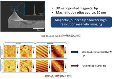
FusionScope magnetic probe and cobalt-iron layer on its surface
Compared with commercial standard magnetic probes
In this paper, we will start from the practical application of FusionScope in the field of magnetism, and explain its powerful functions in the field of magnetic characterization in detail.
Co-characterization of magnetic spintronic nanorods with different components
Ni81Fe19 nanorod assembly was prepared by adjusting the composition ratio, and the morphology was scanned and the AFM and SEM data were accurately correlated, and the magnetic results of three different structures were simultaneously correlated. The magnetic results can clearly distinguish the magnetic distribution of different structures.
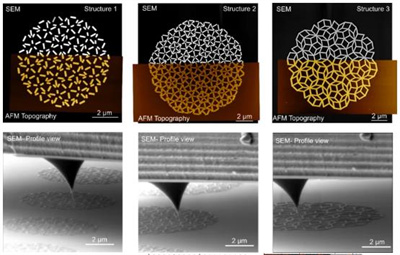
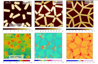
Characterization of Magnetic Properties of Cobalt Layer Etched by FIB
The magnetic properties of cobalt layer are characterized by ion beam etching technology, and the parameters such as magnetic field strength, magnetization curve and magnetic domain structure of cobalt layer are analyzed and evaluated, so as to better understand its magnetic properties.
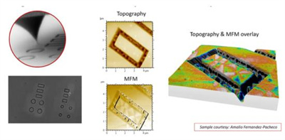
The process or study of magnetic characterization of cobalt layer processed by ion beam etching (FIB) is shown in the figure. The magnetic properties of cobalt layer prepared by ion beam etching technology are analyzed and evaluated. This research may involve measuring the magnetic field strength, magnetization curve, magnetic domain structure and other parameters of cobalt layer in order to better understand the magnetic properties of this material.
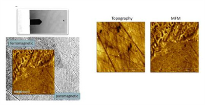
The magnetic properties of industrial steel were characterized.
Duplex stainless steel is a series of stainless steels containing a mixture of austenite and ferrite phases, which can provide higher mechanical strength and ductility than standard steel grades. The grain boundary of duplex stainless steel can be observed and selected by using the SEM of FusionScope, and the AFM probe locates the probe at the grain boundary of two phases according to the information of SEM, and the magnetic structure of the sample is characterized. The magnetization curve, hysteresis loop and saturation magnetic induction intensity of steel are measured to better understand the magnetic properties of industrial steel. This information is of great significance for evaluating the quality of steel, magnetic application and detection methods.
Application advantages of FusionScope combining SEM and MFM
Multidimensional comprehensive characterization
Simultaneous measurement of morphology and magnetism: when SEM provides high-resolution morphology images of samples, MFM can provide magnetic information at the same time to realize the integrated characterization of sample structure and magnetism, which is very important for studying the structure-performance relationship in magnetic materials and devices.
Synchronous imaging: SEM and MFM images can be obtained at the same time, and the surface morphology and magnetic distribution of samples can be observed at the same time in the same accurately matched area, which is helpful to understand the physical properties of complex materials and structures more deeply.
Combination of high resolution and deep depth of field
High-resolution morphology and magnetic imaging: SEM provides morphology images with nanometer resolution, and MFM provides magnetic information with nanometer resolution. The combination of the two can characterize the tiny magnetic structure more accurately, especially when it is necessary to observe the complex three-dimensional structure with high depth of field.
Microscopic magnetic research: For microstructure, such as magnetic domains, magnetic particles or thin films, the integrated system can directly relate the physical morphology and magnetic characteristics of these structures and reveal the internal magnetic interaction.
Efficient analysis
Time saving and data consistency: With simultaneous SEM and MFM imaging, this integrated system reduces the time of sample transfer and switching between different devices, ensures data consistency, and reduces the impact of environmental and operational errors on the results.
Comprehensive analysis of complex samples: for complex samples such as magnetic memory devices and nano-electronic devices, the morphology, composition and magnetism can be comprehensively analyzed in one experiment, which significantly improves the experimental efficiency.
Application field expansion
Research on nano-electronic and magnetic memory devices: For the research of nano-electronic devices, magnetic memory devices and other high-tech fields, this integrated system can provide all-round analysis from morphology to magnetic distribution, and help to develop and optimize new functional materials and devices.
Multi-physical field research: under the action of magnetic field, electric field, stress and other external fields, the morphology change and magnetic response of the sample can be observed simultaneously, which provides a new means for studying the multi-physical field coupling behavior of materials.